Since I've already developed a reliable process for reflowing 0402 surface mount components, as well as 1mm pitch BGA, the next logical step was 0201 passives.
I made a 1x1 inch test board with a bunch of 0201 footprints plus several other test structures (I hope to fool with homebrew filled vias at some point so I included an 0.8mm BGA with drilled-out pads on the same dummy board) on DorkbotPDX's batch order. When I eagerly opened my purple envelope late last month I was quite annoyed to discover that my soldermask pattern was completely wrong!
 |
| Soldermask bugs |
The component values on the silkscreen were a screwup on my part but the fab had totally borked the mask. The correct pattern had the via fence unmasked and all of the areas around components masked.
After emailing back and forth with Laen we figured out the problem - my soldermask polygon had gone slightly outside the board outline and a bug in his panelization script resulted in the offending vertex being deleted, rather than clamped to the board outline. He offered to make me a new batch of boards at no cost.
The new boards arrived today and I inspected them briefly under the microscope. As usual they were superb quality, with near-perfect registration between layers.
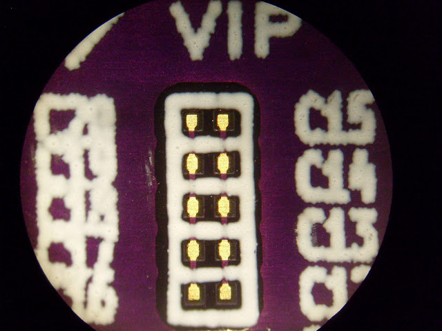 |
| Pre-assembly inspection of 0201 footprints |
My first attempt at applying solder paste using a 22 gauge needle was a complete failure. There was as much paste between the pads as on them.
 |
| Somehow I don't think this will work... |
I tried scraping the paste around with a scalpel blade and managed to get something halfway decent, but it still wasn't nearly as clean as I wanted. After thinking for a bit I decided to try squirting paste onto a microscope slide, then picking up a tiny blob with the blade and touching it to the component pads. This actually worked out surprisingly well!
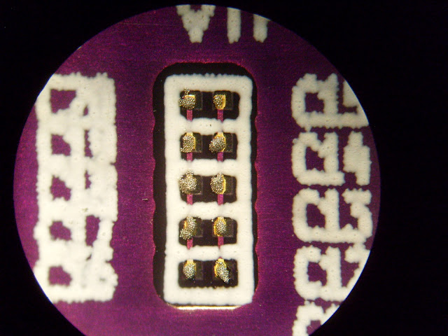 |
| Paste applied with scalpel blade |
I wasn't expecting to get any better than this (for scale, the traces between the pads are only 150 μm wide) so the next step was to place components.
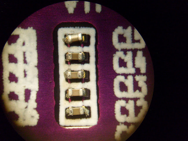 |
| After component placement |
This took a few tries but my super-fine-point tweezers were a huge help. The pitch I used seems to be about the sweet spot - pretty dense, but not so close that my tweezers bang into the next component in line while placing one.
I ran the board through my standard reflow profile in a toaster oven, then inspected.
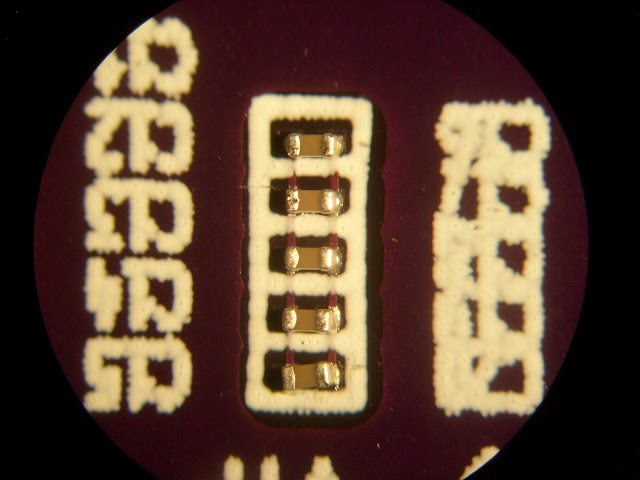 |
| Post-reflow inspection looks good! |
Everything looked good, there were no visible shorts (confirmed by electrical testing) and all connections seemed solid and low resistance. I took a few more photos at varying angles and magnifications to verify.
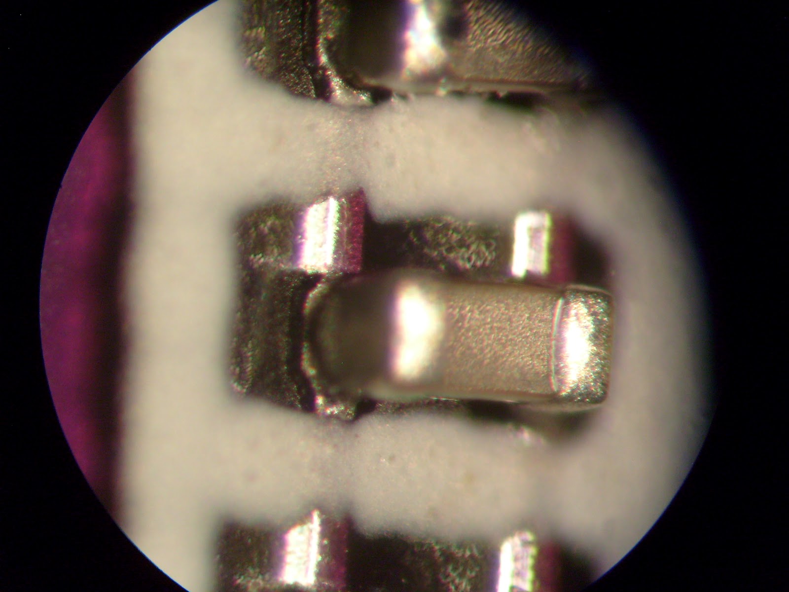
 |
| Angled view of a single component. Note the size of the component in relation to the 35 μm thickness of the 1-ounce copper trace! |
One of these days I need to try using stencils for paste application. In the meantime, it looks like 0201 passives are labor-intensive but definitely within reach for high-density designs.


No comments:
Post a Comment