Most PCBs are patterned using a ferric chloride or copper chloride based etch which is almost perfectly isotropic - it etches equally in all directions. This results in the mask being undercut by approximately the thickness of the copper layer (35 μm for 1oz copper).
 |
| PCB cross section showing sloped sidewalls from undercut (homemade board) |
Ever since I did my first BGA board and noticed some of the pads looked a bit small I've wanted to do a formal study of mask undercut on this process so that I can design future boards with this in mind.
While the undercut is small and insignificant for many applications, it can become a significant issue when working with fine-pitch BGAs, 0201 sized passives, and other very small components!
This was my first time imaging PCBs at high magnifications (more than the 30x of my inspection microscope) so I fooled around a little bit with techniques. Somewhat surprisingly I found that darkfield illumination gave better results than brightfield - brightfield images tended to be far too bright due to reflections from the soldermask.
My first test was one of the leftover boards from my BGA test in January. In darkfield the pads stood out very well and were easy to measure to within a few μm. All dimensions were taken with the focal plane at the top of the trace. At some point in the future I plan to cross-section a board and measure edge profiles.
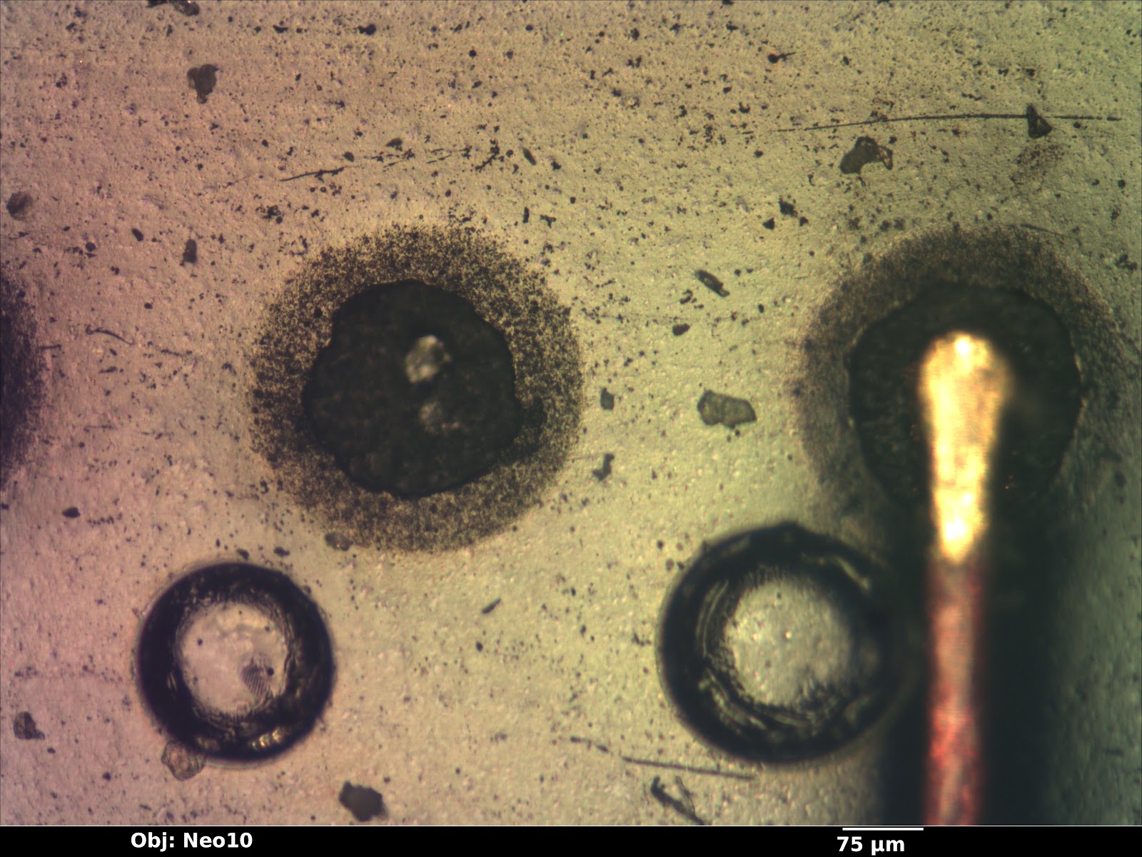
 |
| 200 μm nominal diameter BGA pads (darkfield image). The circles below and to the left of the pads are damage to the soldermask from a misaligned BGA reflow attempt. |
Further inspection showed that one of the isolated pads (not connected to a trace) had been etched away entirely.
 |
| Brightfield image showing empty hole in soldermask where a pad was etched away. Note strong glare from soldermask in brightfield mode. |
A higher magnification image allowed me to measure trace and pad sizes more precisely.
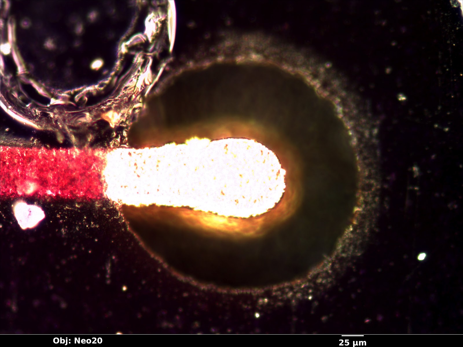 |
| Higher magnification image of same area |
In order to verify that the undercut was not specific to this one board I tried a more recent one - my 0201 passive test panel from last week.
 |
| 0201 capacitor footprint |
 |
| Higher magnification view of a single pad |
The same board also contained an 0.8mm BGA footprint. Pads are nominally 400 μm on 800 μm centers.
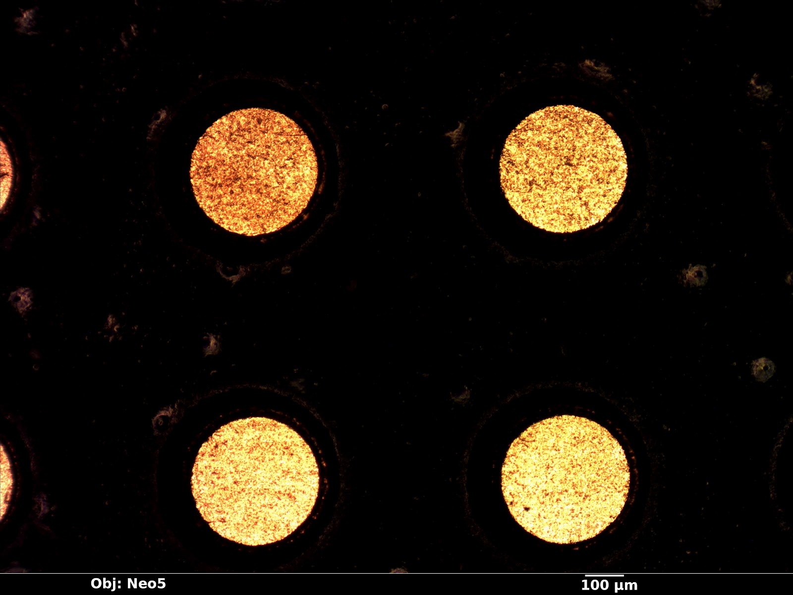 |
| 0.8mm BGA footprint |
In conclusion, the fabricator used by the DorkbotPDX batch order exhibits nontrivial undercut on small features. Observed undercut values ranged from 68 to 133 μm and were fairly consistent within a single board but varied from board to board. The 0.5mm BGA test board exhibited an average undercut of 113.5 ± 19.5 μm and the 0201 test board exhibited an average undercut of 67 ± 4 μm.
No comments:
Post a Comment